Abstract
The proposed research involves the design and implementation of a novel hybrid topology for power quality improvement using multilevel inverter fed induction motor by reducing vibration for Textile applications. Various modern applications have started to require higher power gadgets as of late. Staggered inverter is equipped for giving wanted substituting voltage level at output utilizing different low-level DC voltage as an input. In H-connect staggered inverter, the quantity of output level is characterized by the quantity of exchanged capacitor cells. A small amount of voltage can be utilized to produce a supported output voltage by exchanging the capacitor in parallel and in series. Staggered inverter produces less Total Harmonic Distortion (THD), less electromagnetic interference and less voltage inrush on switches. The proposed topology delivers a staircase waveform with higher number of output level utilizing less segments contrasted with a few existing exchanged capacitor multilevel inverter. The task manages cascaded H-connect staggered inverter that can be utilized for both single and three stage change. The structure is created with H-bridge inverter including DC-DC converter. A sine pulse width twist is decided on PWM pulses. The inverter essentially takes care of the issue of capacitor voltage adjusting as every capacitor is charged to the esteem equivalent to one of the information voltages at each cycle. Recreation is finished with the assistance of MATLAB Simulink programming and the exploratory outcomes for current and voltage at various THD esteems are appeared and the equivalent is done for equipment. The prototype structure is conceded and analysed for various parameters of proposed method, which results in reduced switches and proves more efficient than other conventional methods and in addition it is more proficient for pumping process in textile industry for wastewater treatment.
Highlights
- The source networks having boost abilities are used to step up the voltages from photovoltaic systems and from battery.
- The output voltage can be increased or decreased so that the converter is high reliable.
- The proposed method proves the switches and complex networks present in traditional methods and it is more efficient for pumping process in textile industry.
- The deviation of process parameter value from set point,for overcoming fuzzy controller are proposed.
- Fuzzy controller takes immediate control action by sensing the change of output values.
- The output waveforms with seven steps produces a staircase wave which reduces the harmonic distortion.
1. Introduction
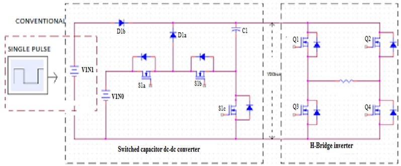
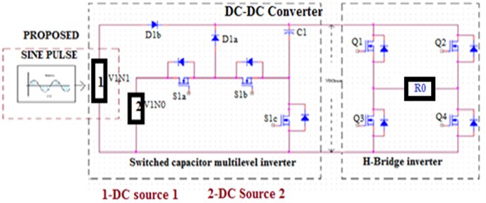
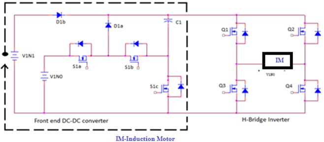
Industrial applications consist of two main areas, motor control and power supplies. The electric utility in industry faces deregulation and characteristic changes are frequently professed. Flexible AC Transmission Systems (FACTS), High-Voltage Direct Current (HVDC) and Custom Power Headway are based on power electronics, which include a fragment of the most encouraging explicit developments, to deal with the new operational difficulties, being revealed today. These degrees of advancement depend upon a superior point of confinement of essentialness electronic mechanical assembly so as to rapidly respond to structure events. So, the addition control trade confines and improves the idea of vitality passed on. In the recent years, the powerful applications are driving the world with the regard of their wide extending thought. Since, various topologies, systems and drive applications are evaluated and examined. Such converters are sensible with high power gadgets dependent on their rating. Reference [1, 2] encircled the staggered power transformation topology with impartial point cinched topology. Ongoing days, the interest in gadgets was related with many quick charging gadgets which outer vitality sources require early examination on consonant and non-dynamic power remuneration [3]. This far reaching symphonious dirtying gadget both lessens the framework effectiveness, and impact affects lattice voltage mutilation levels [4, 5]. Thus, the expansion of flow prompts heat misfortunes and makes a few issues in touchy electrical gadgets. Some ongoing scientists are centered around power quality issues and current music. Power Quality is the best approach to successful movement of value thing and the action of an industry. The growing prominence on the general power system viability realized the use of gadgets, for example, high adequacy, adaptable speed motor drives and shunt capacitors for control factor solution for decline misfortunes achieving extending consonant dimensions on control structures. For different applications like farming and modern diverse topologies of intensity controlled gadgets are intended to insert with the sustainable assets. From this time forward Multilevel inverters (MLIs) are developing as a current logical thing of intensity controlled gadgets for high-control applications. The three noteworthy MLIs are Diode clamped MLI, Flying Capacitor MLI (FC MLI) and Cascaded Single Pulse Staggered Inverters MLI (CSPSI MLI) [6, 7]. CMLI makes the ventured AC voltage waveform with more DC sources with decreased symphonious material. CMLI goes about as a more interesting topology than the other two topology. Cascaded Conventional circuit with single pulse input is shown in Fig. 1.
Fig. 1a) Conventional schematic circuit diagram of single pulse CCSPMLI, b) proposed schematic circuit diagram of CCSPMLI with load R0
a)
b)
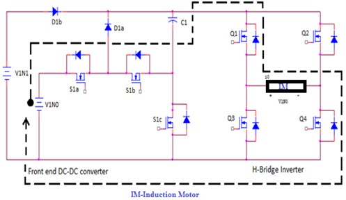
The circuit is fed with the sine pulse and ramp signal for proposed method is shown in Fig. 2. The proposed multilevel inverter is fed with induction motor (MLIFIM).
Fig. 2Schematic circuit diagram with load of MLIFIM
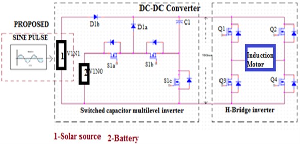
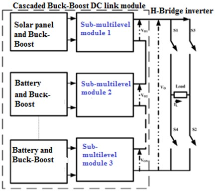
For acquiring output ostensible in CCMLI, new topology staggered converter topology is proposed between the different info sources either thinking about transformer. The productivity and treatment of CCMLI and buck-help CMLI (BBMLIFIM) set ups are degraded as a result of a lot of prohibited power controlled switches and DC sources. The proposed cascaded DC link circuit diagram is shown in Fig. 3.
Fig. 3Proposed structure of Buck-Boost cascaded DC-link multilevel inverter
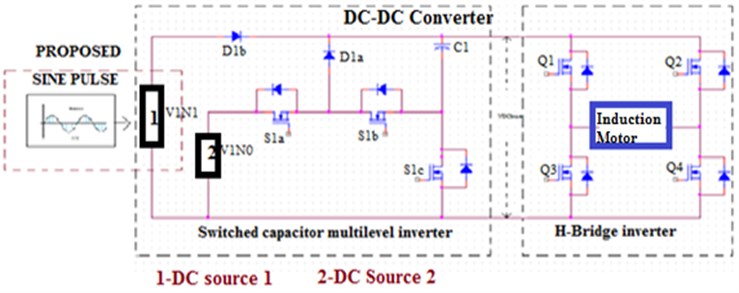
In the interim topological adjustments are made in the current CCMLI [8-12]. From now on in proposed investigate, the buck-boost converter circuit is presented between information sources and DC-connect inverter to acquire ostensible output voltage. Such changes of topology results in the decrease of intensity controlled gadgets advertisement input sources. For this research, a single-stage seven-level and Buck Boost DC-interface CMLI fed induction motor (BBDCCMLIFIM) framework is intended for business applications. Schematic circuit of the proposed BBDCLCMLIFIM framework is appeared in Fig. 4.
To reduce the Total Harmonic Distortion (THD) occurred with the single pulse contribution as proposed [13-16], To overcome this disadvantages, changed sine wave and ramp wave is utilized as an elective strategy in the exploration to lessen the THD and to work the circuit in proficient way. The proposed research is sorted out in six segment: Objectives of Buck-Boost converter is looked into in Section 1. Schematic circuit of BBDCLCMLIFIM framework is described in Section 2. Different exchanging topology have explored in Section 3. Experimental and Mathematical displaying of BBDCLCMLIFIM framework are carried in Section 4, and Section 5 concludes up this paper.
Fig. 4Proposed circuit diagram of BBDCLCMLIFIM with Induction motor
2. Materials and methods
Modeling structure of BBDCLCMLIFIM.
BBDCLCMLIFIM contains double unbalanced DC voltage sources, buck support converter unit, DC-interface module (DCLM) and H-bridge inverter. H-bridge inverter is associated in parallel to the DC-interface framework.
2.1. Buck-boost Cuk DC-link configuration
Buck Boost (BB) converter unit is associated with topsy-turvy DC sources. The identical structure of BDCLMLI is appeared in Fig. 4.
Number of levels in BBDCLCMLIFIM arrangement is determined as:
Number of switches in BDCLCMLI is given by (2):
where is the quantity of levels, is the quantity of switches in BBDCLCMLIFIM, Q-number of H-bridge inverter, S-number of DC sources and P-number of buck-help units.
2.2. Modes of operation
Mode 1: Output voltage = ± state.
Capacitor is charged to the information voltage through by turning ON transistor . Transistors , and diode stay turned off. The DC voltage at this state is equivalent to as is closed by turning off transistor . Voltage source alone supplies capacity to the heap. Fig. 5(a) delineates the identical circuit for V0 = +.
Mode 2: Output voltage = ± state.
For typical activity of the proposed inverter, . In the DC-DC converter, just transistor is turned ON while different transistors are turned off. Consequently, is associated with the DC bus through diode . As , diode is turn around one-sided and henceforth squares . Fig. 5(b) delineates the proportionate circuit for . The capacitor is open at this state. Along these lines, its voltage stays at .
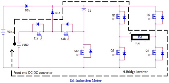
Fig. 5Operating modes of proposed BBDCLCMLIFIM
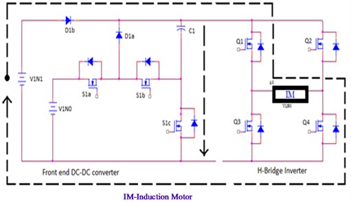
a) IM-Induction motor
b)
c)
d)
Mode 3: Output voltage = ±() state.
Capacitor charged to , is associated in arrangement with info voltage source by turning ON transistors and . Diode is turn around one-sided and blocks . The net voltage that shows up over the DC transport currently is equivalent to . In this state, input voltage source and capacitor supply capacity to the heap. Fig. 5(c) delineates the proportionate circuit for .
Mode 4: Output voltage = 0 V state.
To acquire zero dimension at the output after the positive half cycle Fig. 5(d), just transistor is turned ON, while the various switches in the H-bridge inverter stay killed. The diode of transistor is utilized for nothing wheeling. Essentially, to get zero dimension at the output after the negative half cycle, just transistor is turned ON, while the various switches in the full scaffold inverter stay turned off. For this situation, the diode of transistor is utilized for freewheeling. The switches in the front-end converter stay in their past states.
(a) Mode 1: Output voltage = ± state (b) Mode 2: Output voltage = ± state.
(c) Mode 3: Output voltage = ±() state (d) Mode 4: Output voltage = 0 V state.
At Output voltage = ±, the net voltage that shows up over the DC transport currently is equivalent to .
The output voltage is communicated as:
At right now charging vitality is given as:
The normal output voltage of buck help converter can be communicated utilizing Eq. (5):
The vitality discharged by the circuit at switch s1a by the proposed converter given by Eq. (6):
The proposed converter BB with lessening exchanging misfortunes are communicated in condition Eq. (7):
Voltage variety over the capacitor C1 can be communicated by Eq. (8):
Operation modes 3 and 4: Capacitor charged to , is connected in series with input voltage source by turning ON transistors and . Diode is reverse biased and blocks . To obtain zero level at the output after the positive half cycle only transistor is turned ON, while all the other switches in the H-bridge inverter remain turned OFF. The diode of transistor is employed for free-wheeling. Similarly, to obtain zero level at the output after the negative half cycle, only transistor is turned ON, while all the other switches in the full extension inverter stay turned off. The net voltage that shows up over the DC transport currently is equivalent to . are appeared in Fig. 5(c) and 5(d).
Capacitor charged to , is associated in arrangement with info voltage source by turning ON transistors and the present changes from to . The voltage over the inverter circuit is communicated as:
The vitality discharged by the circuit at switch by the proposed converter given by Eq. (10):
The normal output voltage of buck help converter II is acquired utilizing Eq. (11):
The proposed converter BB with lessening exchanging misfortunes are communicated in condition Eq. (12):
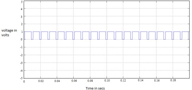
A model of single-stage BBDCLCMLIFIM-based engine is structured and executed for 230 V () output voltage. The examples of PWM pulses, Simulink display and the output voltage utilizing n-levels are appeared in Figs. 6(a) and (b).
Fig. 6a) PWM pulses, b) topology of a flying capacitor multilevel inverter
a)
b)
Rectifier units, buck boost converter units, controller units, driver units, DC-connection and H-bridge inverter units are incorporated in this model. The rectifier units are planned utilizing a scaffold rectifier (MICBR1010) and a capacitive channel of 1000 μF. The outputs of rectifier units go about as the contribution for the lift chopper units and battery banks. The buck support converter are manufactured utilizing IRF840 controlled power gadgets (MOSFET) switches and aloof segments ( 100 μF). The dspic gives control signs to the MOSFET driver circuit. The highlights of dspic are utilized to accomplish effective control of the proposed framework. The DCLM and H-bridge inverter frameworks are manufactured utilizing IRF840 control MOSFET switches. The experiment identical circuit of BBDCLCMLIFIM framework is appeared in Fig. 22. Output voltage across capacitor can be expressed by (13):
Table 1Switch turning states of BBDCLCMLIFIM with respect to potential rating
Potential rating, Volts | State level | Switch turning states | |||||||||||||
– | |||||||||||||||
+4 | 1 | 0 | 1 | 0 | 1 | 1 | 0 | 1 | 0 | 1 | 0 | 1 | 0 | 1 | 0 |
+3 | 2 | 1 | 0 | 0 | 1 | 1 | 0 | 1 | 0 | 1 | 0 | 1 | 1 | 0 | 0 |
+2 | 3 | 1 | 0 | 0 | 1 | 1 | 0 | 1 | 1 | 0 | 1 | 1 | 0 | 1 | 0 |
+1 | 4 | 0 | 1 | 0 | 1 | 1 | 0 | 1 | 1 | 0 | 1 | 1 | 1 | 0 | 0 |
+0 | 5 | 1 | 0 | 0 | 1 | 1 | 0 | 1 | 1 | 0 | 1 | 0 | 1 | 0 | 1 |
–0 | 6 | 1 | 1 | 1 | 0 | 1 | 0 | 1 | 1 | 0 | 1 | 1 | 0 | 1 | 0 |
–1 | 7 | 0 | 1 | 1 | 0 | 1 | 0 | 1 | 1 | 0 | 1 | 1 | 1 | 0 | 0 |
–2 | 8 | 1 | 1 | 1 | 0 | 1 | 0 | 1 | 1 | 0 | 1 | 0 | 1 | 0 | 1 |
–3 | 10 | 0 | 1 | 1 | 0 | 0 | 1 | 0 | 1 | 0 | 1 | 1 | 1 | 0 | 0 |
–4 | 11 | 1 | 0 | 1 | 0 | 0 | 1 | 0 | 1 | 0 | 1 | 0 | 1 | 0 | 1 |
+4 | 12 | 1 | 0 | 0 | 1 | 1 | 0 | 1 | 0 | 1 | 0 | 1 | 0 | 1 | 0 |
+3 | 13 | 1 | 1 | 0 | 1 | 1 | 0 | 1 | 0 | 1 | 0 | 1 | 1 | 0 | 0 |
2.2.1. Operation of H-bridge inverter configuration
The output voltage before H-bridge inverter for single PWM pulse is appeared in Fig. 9. It delivers a most extreme voltage of total of and . At present, a couple of topologies with various control systems have been presented for cascaded staggered inverters. This exploration considered this connects idea and executed in this framework. H-bridge inverter framework works in two activity modes. The positive half-cycle sizes of AC output voltage are communicated utilizing Eqs. (14)-(16):
At MODE (b), the contrary half cycle of AC output voltage is incorporated by stimulating H-connect control gadgets and as appeared in Fig. 5(b) and (d).
The negative half cycle extents of AC output voltage are given by:
2.2.2. Buck boost converter conduction losses
With reference MOSFET switching losses are determined utilizing the exact voltage drop with arrangement straight resistor ( 0.07). It decides the terminal entryway by terminal source voltage and intersection temperature. The misfortunes in the MOSFET switch are given in Eq. (19).
on:
where () shows the present coursing through the switch (), () represents the “ON” time of switch and delta represents the normal swell current of switch. Exchanging ampere decided as () is gotten from Eq. (20). Initial current are given as in Eq. (20):
where () and () gives high and low sizes of intensity controlled gadget current (-) as outlined in Fig. 7. From Fig. 8, 0.22, 7.565 and 0.965, which are substituted in Eq. (21), total ripples and losses are gotten from MOSFET switches [18] as settled and conduction losses are determined in Eq. (21), (22):
Power devices conveyance losses () during starting.
Fig. 7Conduction of power devices at open loop condition [18]
![Conduction of power devices at open loop condition [18]](https://static-01.extrica.com/articles/19896/19896-img12.jpg)
3. Results and discussions
3.1. Simulation performance evaluation
The designed control topology is striving with a perfect three-stage connection with a two-phase BBC power supply and an induction motor. Table 2 shows the simulation specifications, which supports in reducing the harmonic distortion.
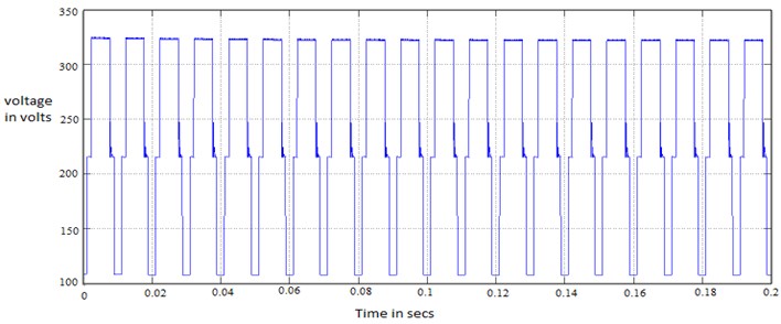
3.2. Output voltage before H-bridge inverter for single pulse
The output voltage before H-bridge inverter for single PWM pulse is shown in Fig. 9. It produces a maximum voltage of sum of and .
3.3. Output voltage and current for single PWM pulse
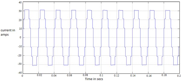
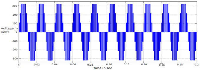
The output voltage and current of multilevel inverter for single pulse input is shown in Fig. 10 and Fig. 11.
Fig. 8Converter: a) diode conduction losses b) ripple currents across inductor, diodes and capacitor [17]
![Converter: a) diode conduction losses b) ripple currents across inductor, diodes and capacitor [17]](https://static-01.extrica.com/articles/19896/19896-img13.jpg)
a)
![Converter: a) diode conduction losses b) ripple currents across inductor, diodes and capacitor [17]](https://static-01.extrica.com/articles/19896/19896-img14.jpg)
b)
Table 2Simulation specifications
PARAMETERS | UNITS |
Solar PV voltage | 24 V |
Solar PV current | 2.20 A |
Solar PV power | 74 W |
FET resistance () | 0.1 Ω |
Internal diode resistance () | 0.01 Ω |
Internal diode inductance () | 1 H |
Internal diode forward voltage () | 1 V |
Initial current () | 0.1 A |
Snubber resistance () | 1×10⁻⁵ Ω |
Snubber capacitance () | 1 nF |
Inductance () | 1 H |
Forward voltage () | 0.8 V |
Initial current () | 1 A |
Snubber resistance () | 500 Ω |
Snubber capacitance () | 250×10-9 nF |
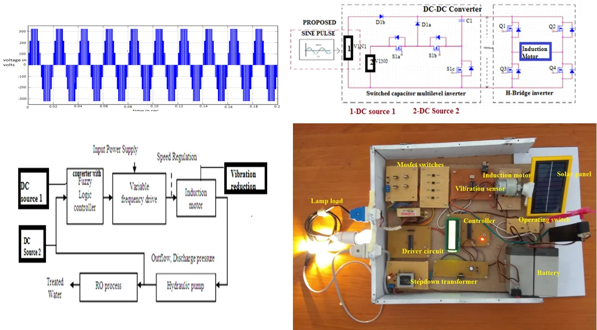
The output waveform with seven steps produces a staircase wave which reduces the harmonic distortion. Single pulse multilevel inverter is an existing system. To improve the performance the single pulse is replaced by sine pulse. Our proposed system has sine signal compared with ramp signal as an input pulse. It reduces harmonic distortion than single pulse. The simulation outputs for sine pulse are given below. The multilevel inverter switches receives the converter outputs. The recreation parameters of the designed model are set as follows: input voltage = 480 V, input current = 27 A, input supply frequency = 50 Hz, exchanging frequency = 2 kHz, resistance =20 Ω and inductance = 310 mH for 7 level inverter. The output voltages are synthesized using the MATLAB platform. Multilevel inverters with 7-levels output voltage synthesis are shown in Fig. 13, 14 and 15.
Fig. 9Output voltage before H-bridge inverter
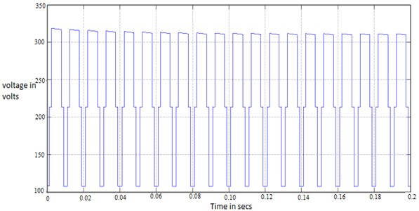
Fig. 10Output voltages after H-bridge inverter
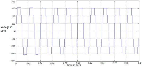
Fig. 11Output current after H-bridge inverter
3.4. Voltage across capacitor for sine pulse
Capacitor gets charged and maintains it ideally and then it gets discharged. The voltage across the capacitor for sine pulse modulation is shown in Fig. 12.
3.5. Output voltage before H-Bridge inverter
The output voltage before H-bridge inverter for sine PWM pulse is shown in Fig. 13. It produces a maximum voltage of sum of and .
Fig. 12Voltage across capacitor for sine PWM
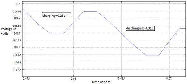
Fig. 13Output voltage before H-bridge inverter
3.6. Output voltage and current for sine PWM pulse
The output voltage and current of multilevel inverter for sine pulse input is shown in Fig. 14 and Fig. 15.
The output waveform with seven steps produces a staircase wave which reduces the harmonic distortion.
Fig. 14Output voltage after H-bridge inverter
3.7. THD analysis
The THD % for single pulse and sine pulse at modulation index 1 are shown in Fig. 16.
THD for various modulation indices.
The comparisons of THD percentage of single pulse and sine pulse for different modulation indices are tabulated in Table 3.
Fig. 15Output current after H-bridge inverter
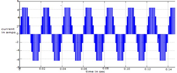
Fig. 16a) THD results for single pulse, b) THD results for sine pulse
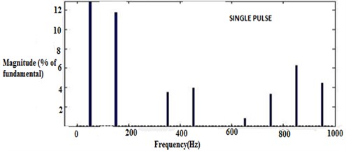
a) Fundamental (50 Hz) = 367.9 THD = 17.08 %
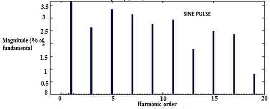
b) Frequency (50 Hz) = 282.1 THD = 8.11 %
Table 3Comparison of THD percentage of single pulse and sine pulse for different modulation indices
Sl. No | Modulation index | Conventional | Proposed |
THD % | THD % | ||
1 | 1.2 | 20.64 | 8.45 |
2 | 1.1 | 18.85 | 8.80 |
3 | 1 | 17.08 | 8.11 |
4 | 0.9 | 15.84 | 8.33 |
5 | 0.8 | 16.30 | 10.63 |
6 | 0.7 | 20.99 | 14.94 |
7 | 0.6 | 23.95 | 14.24 |
9 | 0.4 | 28.98 | 20.36 |
10 | 0.3 | 48.32 | 18.17 |
3.8. Analysis of speed regulation in pumping process of RO section in textile wastewater treatment
The block diagram of speed control system is shown in the Fig. 17.
The pumping process parameters, pressure and flow are optimized by adjusting the electrical parameters, duty cycle and speed. The proposed Fuzzy Logic Control (FLC) system has two inputs: the first input is the difference in actual and desired flow; the second input is the difference in actual and desired pressure. FLC is applied to the speed controlling system to control the speed of the induction motor. The output of FLC is sent to the three-phase inverter to produce waveform with variable frequency to control the speed of the three phase induction motor. For fuzzy logic controller, ranges for membership functions have to be defined. The range of input variables pressure (PR), flow (FL) and output variable duty cycle are defined as Negative Large (NL), Negative Medium (NM), Negative Small (NS), Zero (ZE), Positive Small (PS), Positive Medium (PM), Positive Large (PL). The output variable is used to calculate the needed change of frequency which will be used to control the speed of induction motor. All fuzzy rules used in the proposed system are summarized in the Table 4.
Fig. 18 shows the fuzzy membership function of fuzzy controller for speed controlling system with inputs and output of the system.
Table 5 shows the variation of electrical parameter values with respect to process parameters.
Fig. 17Block diagram of speed control system
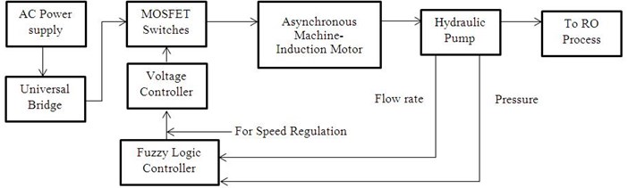
Table 4Fuzzy rules for speed control system
PR | NL | NM | NS | ZE | PS | PM | PL |
FL | |||||||
NL | NB | NB | NB | NB | NM | NS | ZE |
NM | NB | NB | NB | NM | NS | ZE | PS |
NS | NB | NB | NM | NS | ZE | PS | PM |
ZE | NB | NM | NS | ZE | PS | PM | PB |
PS | NM | NS | ZE | PS | PM | PB | PB |
PM | NS | ZE | PS | PM | PB | PB | PB |
PL | ZE | PS | PM | PB | PB | PB | PB |
Table 5Variation of electrical parameter values with respect to process parameters
Outflow of liquid from pump (gpm) | Discharge pressure of liquid from pump (psi) | Duty cycle for inverter | Speed of induction motor (rpm) |
400 | 21 | 0.1 | 1750 |
219 | 18.67 | 0.2 | 1051 |
188 | 15.98 | 0.3 | 900 |
100 | 11 | 0.5 | 690 |
Whenever there is a deviation of process parameter value from set point, fuzzy controller takes immediate control action by sensing the change of values. By changing the duty cycle, frequency of the supply that is fed to the inverter is varied. Consequently, the rotor speed can be varied. Instead of running the motor at full frequency of 50 Hz during the entire day, the frequency can be reduced when the load reduces, and energy consumption can be reduced. Fig. 19 shows the rotational speed of rotor in rpm. The speed of the motor obtained for the corresponding pressure and flow is 900 rpm.
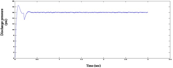
Fig. 20 and Fig. 21 shows the discharge flow rate and discharge pressure of the pumping process. The obtained flow and pressure values are 188 gpm and 15.98 psi for 900 rpm.
Fig. 18Membership function for speed controller
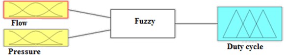
Fig. 19Rotor speed of the motor
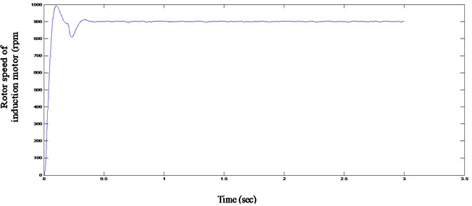
Fig. 20Discharge flow rate of the pump
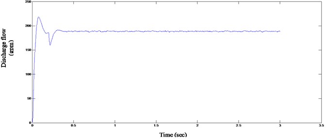
Fig. 21Discharge pressure of the pump
Whenever there is a deviation of process parameter value from set point, fuzzy controller takes immediate control action by sensing the change of values. By changing the duty cycle, frequency of the supply that is fed to the inverter is varied. Consequently, the rotor speed can be varied. Instead of running the motor at full frequency of 50 Hz during all the day, the frequency can be reduced when the load reduces, and energy consumption can be reduced.
3.9. Experimental evaluation
The converter outputs are encouraged to staggered inverter switches for the application for the material water siphoning process with the fluffy rationale controller. The experimental parameters are set as pursues: supply recurrence = 50 Hz, input voltage = 480 V, input current = 27 A, trading recurrence = 2 kHz, opposition = 20 Ω, inductance = 310 mH. Table 6 demonstrates engine parameters. The acknowledgment equipment circuits are appeared in Fig. 22. Block diagram and Prototype Model equipment of BBDCLCMLIFIM appeared in Fig. 23 and 24. The structured BBDCLCMLIFIM analysis were carried out and hence the proposed method achieves reduced THD which is more cost effective and efficient for the various industry applications.
Fig. 22Realization of hardware circuit diagram of BBDCLCMLIFIM
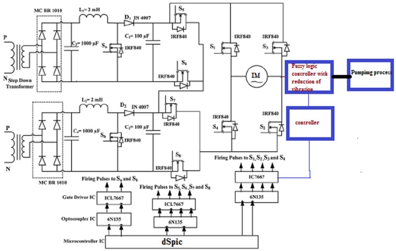
Table 6Various type of equipment with their range specification
S. No | Type of the equipment | The range |
1 | Battery | 12 V/4.7 AH |
2 | Step down transformer | 230 V/12 V |
3 | Step down transformer | 230 V/5 V |
4 | MOSFET | IRF840 |
5 | Induction motor | 220 V, 100 A, 1200 rpm |
Table 7Comparison of THD for various multilevel inverters to reduce vibration across the induction motor
Parameter | Diode clamped | Developed H bridge | Torque ripple | Current ripple |
Proposed THD for level 7 (%) | 17.08 | 8.11 | 0.6 | 0.7 |
THD for level 5 (%) | 15.84 | 8.33 | 0.66 | 1.2 |
THD for level 3 (%) | 16.30 | 10.63 | 0.71 | 1 |
THD for level 2 (%) | 20.99 | 14.94 | 0.89 | 1.6 |
Fig. 23Experimental block diagram of BBDCLCMLIFIM
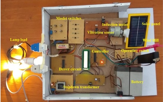
Fig. 24Prototype hardware of BBDCLCMLIFIM with vibration sensor for pumping applications in textile wastewater treatment
4. Conclusions
The hybrid quasi converters with solar and battery sources are incorporated in the proposed subsystem, for analysis and design. The task manages cascaded H-connect staggered inverter that can be utilized for both single and three stage change. The structure is created with H-bridge inverter including DC-DC converter. A sine pulse width twist is decided on PWM pulses. The inverter essentially takes care of the issue of capacitor voltage adjusting as every capacitor is charged to the esteem equivalent to one of the information voltages at each cycle. Recreation is finished with the assistance of MATLAB Simulink programming and the exploratory outcomes for current and voltage at various THD esteems are appeared and the equivalent is done for equipment. The proposed method is designed with 7-level diodes clamped based on the converter unit. The H bridge topology was developed with MATLAB/Simulink. Finally, the operation of total subsystem is verified based on the harmonic reduction. From the experimental results, it is concluded that the proposed subsystem with the developed H bridge converter has the least total harmonic distortion as 8.11 % and 17.08 % for 7-level and 5-level MLI topology respectively. The prototype structure is conceded and analysed for various parameters of proposed method, which results in reduced switches and proves more efficient than other conventional methods and in addition it is more proficient for pumping process in textile industry for wastewater treatment.
References
-
Li Z., Wang P., Li Y., Gao F. A novel single-phase five-level inverter with coupled inductors. IEEE Transactions of Power Electronics, Vol. 27, Issue 6, 2012, p. 2716-2725.
-
Najafi E., Yatim A. H. M. Design and implementation of a new multilevel inverter topology. IEEE Transactions of Industrial Electronics, Vol. 59, Issue 11, 2012, p. 4148-4154.
-
Junfeng Liu, Cheng K. W. E., Ye Y. A cascaded multilevel inverter based on switched-capacitor for high-frequency AC power distribution system. IEEE Transactions of Power Electronics, Vol. 29, Issue 8, 2014, p. 4219-4230.
-
Sathishkumar Shanmugam, Mahendran Krishnamoorthy, Meenakumari Ramachandran, Krishnakumar Kanagaraj Solar power based DC-DC converter fed brushless DC motor drive for agricultural applications. Indian Journal of Ecology, Vol. 45, Issue 1, 2018, p. 25-32.
-
Abd Elazim S.-M., Ali E. S. Hybrid particle swarm optimization and bacterial foraging for power system stability enhancement. Complexity, Vol. 21, Issue 2, 2015, p. 245-255.
-
Zhijun E., Fang D. Z., Chan K. W., Yuan S. Q. Hybrid simulation of power systems with SVC dynamic phasor model. International Journal of Electrical Power and Energy Systems, Vol. 31, Issue 5, 2009, p. 175-180.
-
Suresh Balasubramaniam, Saravanakumar Gunasekaran, Sampathkumar Ramasamy, Sathish Kumar Shanmugam Design and implementation of solar power fed permanent magnet synchronous motor with improved DC-DC converter and power quality improvement using shunt active filter for reducing vibration in drive for industrial applications. Journal of Vibroengineering, Vol. 21, Issue 2, 2019, p. 507-525.
-
Hariri A., Faruque M. O. Hybrid simulation tool for the study of PV integration impacts on distribution networks. IEEE Transactions on Sustainable Energy, Vol. 8, Issue 2, 2017, p. 648-657.
-
Yilmaz M., Krein P. T. Review of battery charger topologies, charging power levels, and infrastructure for plug-in electric and hybrid vehicles. IEEE Transactions on Power Electronics, Vol. 28, Issue 5, 2013, p. 2151-2169.
-
Shuai Z., Liu D., Shen J., Tu C., Cheng Y., Luo A. Series and parallel resonance problem of wideband frequency harmonic and its elimination strategy. IEEE Transactions on Power Electronics, Vol. 29, Issue 4, 2014, p. 1941-1952.
-
Odeh C. I., Anih L. U., Ejiogu E. C. 17-Level switched voltage source multi-level inverter topology with low-switching frequency control. Electric Power Components and Systems, Vol. 44, Issue 19, 2016, p. 2185-2197.
-
Odeh C. I. Improved three-phase, five-level pulse-width modulation switched voltage source inverter. IET Power Electronics, Vol. 8, Issue 4, 2015, p. 524-535.
-
Salmon J., Knight A. M., Ewanchuk J. Single-phase multilevel PWM inverter topologies using coupled inductors. IEEE Transactions of Power Electronics, Vol. 24, Issue 5, 2009, p. 1259-1266.
-
Ho A. V., Chun T. W. Single-phase modified quasi-Z-source cascaded hybrid five-level inverter. IEEE Transactions on Industrial Electronics, Vol. 65, Issue 6, 2018, p. 5125-5134.
-
Senthilkumar Arumugam, Sathish Kumar Shanmugam, Anbarasu Loganathan, Gowtham Palanirajan, Meenakumari Ramachandran A novel bridged-insert cascaded five level inverter topology. Journal of Measurements in Engineering, Vol. 6, Issue 4, 2018, p. 297-310.
-
Bharatiraja C., Ravi A., Banerjee S., Chakraborty A., Anupam A., Menon A. Hybrid cascaded multilevel inverter with diode assisted boosting network. Energy Procedia, Vol. 117, 2017, p. 1024-1031.
-
Shanmugam S., R. Meena Kumari Design and implementation of modified buck boost converter fed B4 inverter for brushless DC motor drive using low cost DSPIC controller. Asian Journal of Research in Social Sciences and Humanities, Vol. 6, Issue 10, 2016, p. 1079-1101.
-
Shanmugam S., Ramachandran M., Kanagaraj K., Loganathan A. Sensorless control of four-switch inverter for brushless DC motor drive and its simulation. Circuits and Systems, Vol. 7, Issue 6, 2016, p. 726-734.
-
Sathish Kumar Shanmugam, Arumugam Senthilkumar Design and implementation of DC source fed improved dual-output buck-boost converter for agricultural and industrial applications. Journal of Vibroengineering, Vol. 19, Issue 8, 2017, p. 6433-6454.
About this article

